


As semiconductor technology advances, the importance of design is growing even more. This is because design plays the decisive role in fitting more features onto a smaller area while balancing the trade-off between high performance and low power. Defining the functions of a semiconductor and designing the circuits that act as its brain, the Design role is the starting point of the journey for a single product, and it is no exaggeration to call it the start of all technical challenges. The Newsroom, together with Student Ambassadors of SK hynix, Kyungtae Kim and Yunjin Kim, met with Jongseok Kim (TL, DRAM Design) and Minchul Shin (TL, NAND Design Team) to hear about the role and value of design, and the competencies required to perform the job.


Building the Brain of Semiconductors with Logic and Circuits—Design
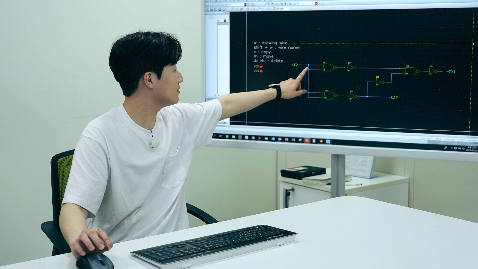
Design is about implementing the required functions a semiconductor using ‘logic’ and ‘circuits.’ To use a construction analogy, it corresponds to designing a blueprint tailored to the building’s purpose and structure. In other words, it is the process of defining the direction of product development by determining what functions will be realized with what structures, and how to arrange the necessary devices to achieve this. The design roles are largely divided into Circuit Design and Digital Design. Circuit Design creates various circuit elements that enable the product to operate. It encompasses the entire process from advanced technology research, product circuit design, circuit analysis and verification, competitor analysis, yield enhancement and development methodology improvement, to developing enabling technologies for future products. Digital Design drafts digital circuit blocks with specific functions, known as Intellectual Property (IP). The key is optimizing complex conditions such as Power, Performance, and Area (PPA) to meet the customer requirements on performance and specifications. Design engineers from two different parts collaborate closely from the initial design phase, jointly defining and applying the architecture and operational methods of the product. Because circuits are defined at different levels according to chip characteristics and requirements, it takes diverse perspectives and technologies to make the final product. Design is completed through a seamless workflow of three steps: Schematic Design, Layout Design, and Verification. First, schematic design logically defines and implements product functions. Then, layout design converts them into a physical structure, so it can actually be built onto the semiconductor. Finally, at the verification phase, the circuit operations are evaluated and improved through simulation. Above all, Design involves high-level work that goes beyond simple circuit composition; it requires comprehensive judgment and coordination of performance, stability, and manufacturability. To derive the optimal design plan amidst various technical constraints and variables, numerous iterations and discussions are required, and the product robustness is elevated through close collaboration with various teams in the areas of Process, Device and Test.

Who We’re Looking For
As the semiconductor industry faces the limits of scaling and the rise of SoC*, the complexity and importance of design continue to grow. In this environment, design roles are evolving beyond the technical task of simply designing circuits into a core business function—planning and implementing products that can succeed in the market. * SoC (System on Chip): A type of semiconductor in which various functions, such as CPU, GPU, and memory, are integrated into a single chip. To perform a design role, it is essential to have foundational capabilities in understanding and working with logic and circuits—the basic language of design. This is why design positions tend to have a higher proportion of candidates from related fields such as electronics, semiconductors, physics, and computer engineering compared to other roles. However, academic background does not determine everything. Since practical capabilities can be developed sufficiently through learning and experience after joining the company, what matters even more are logical thinking, perseverance, and detail-oriented focus. These are the capabilities required throughout the work process: logically analyzing complex computational structures, persistently identifying even the smallest errors, and improving the design to enhance its completeness. In addition, because dozens of engineers collaborate toward a single outcome, the ability to embrace diverse perspectives and communicate smoothly is also important. “Design is the first step that determines the functionality of a semiconductor product, and it plays a key technical role in realizing high-performance, high-efficiency products,” said Sangmok Song (TL, Talent Acquisition). “As a result, the ability to reflect customer needs and market trends in design is becoming increasingly important.” He added, “Design is a demanding field, but for those who are determined to see things through to the end, it is also one of the most rewarding roles. If you are interested in next-generation semiconductor design at SK hynix, a ‘Full Stack AI Memory Provider,’ I encourage you to take on the challenge.”


Q1. Could you briefly introduce yourselves?
Jongseok Kim (TL): I am Jongseok Kim from the DRAM Design Team. I am responsible for layout design, physically implementing the analog circuits that transmit and receive data between chips. As DRAM continues to become faster and denser, we are exploring various ways to enhance layout design quality to optimize interface characteristics while staying within process limitations. Minchul Shin (TL): I am Minchul Shin from the NAND Design Team. I am responsible for the design and verification of the PDN*, or Power Distribution Network, which manages the power network across the entire chip. Our key focus is ensuring power integrity so that major circuits can operate reliably. To achieve this, we design structures that efficiently distribute and control power across all blocks within the chip. * PDN, Power Distribution Network: A power delivery path designed to supply stable and uniform power to circuits within a chip. It is a critical element for high-speed signal processing and low-power implementation.
Q2. What are the core values and goals of the design role?
Jongseok Kim (TL): Design goes beyond simply implementing given specifications. Our goal is to create high-quality products that satisfy multiple, often competing conditions such as productivity, quality, low power consumption, and high-speed performance. To achieve this, we relentlessly pursue continuous improvement and innovation. Minchul Shin (TL): I believe the fundamental goal of design is to create chips that are smaller, more stable, and higher-performing. In the context of NAND design, our long-term objective is ultimately to produce SSDs (Solid State Drives) that are cost-competitive enough to replace HDDs (Hard Disk Drives).
Q3. What is the biggest challenge you face in your role?
Jongseok Kim (TL): Finding the optimal solution among conflicting requirements like high performance, low power, and high density. This is particularly challenging in interface circuit design, where we must secure high-speed characteristics while minimizing signal and power degradation through precise layout design. Minchul Shin (TL): Recently, CSR* and power reduction have become major issues. As more customers demand low-power NAND products, we are exploring various new design approaches different from conventional methods. To adapt to these changes, close collaboration among design engineers across different fields is more critical than ever. * CSR (Chip Size Reduction): A design strategy aimed at reducing the overall chip area to lower costs and achieve higher integration.
Q4. What qualities or competencies are most essential for the design role?
Jongseok Kim (TL): A solid understanding of circuits is the foundation of design. Based on this, you must be flexible in finding solutions for various problems. On a macro level, it is crucial to predict potential defects, while on a micro level, meticulousness is required to minimize errors. Even a small mistake can impact the entire schedule and product quality. Minchul Shin (TL): In design, a single number can change the outcome, and a minor error can delay the development schedule by several months. Therefore, meticulousness is very important. Furthermore, solving one problem often requires a number of reviews. In this process, “persistence”—the drive to dig deep without giving up—is also a crucial quality.
Q5. What advice would you give to prospective applicants aspiring to work in Design?
Jongseok Kim (TL): Design work might seem daunting, but rather than focusing on knowledge or immediate achievements, steadily building a strong foundation is far more beneficial for your career. Specifically, for DRAM design roles, the company provides an in-person group training program called “Design School” for newcomers. There, you can systematically learn the entire workflow—from circuit design and layout design to verification—directly from senior engineers. This program is designed to equip you with the practical skills needed to handle tasks immediately upon team placement. Above all, I believe the most important thing is to maintain curiosity about everything and adopt an attitude of self-driven learning by asking your own questions. Minchul Shin (TL): I also thought design was difficult as a student. However, through the onboarding training programs, I was able to adapt well. You don’t have to be an expert to join our team. If you are interested and passionate, this is a field worth trying. I encourage you to bring up the courage and take the first step.