


Before a next-generation semiconductor can be successfully mass produced, extensive process development must first be carried out to verify and optimize numerous conditions. The key role in this process is played by the R&D Process team. What roles do R&D process members play as they connect design and mass production to bring next-generation semiconductor technologies to life? And what competencies are required to succeed in this role? The Newsroom, alongside Student Ambassadors of SK hynix, Sujin Lee and Seunghyun Bang, spoke with Jieun Kim (TL, N-PMA) and Byul Choi (TL, Wafer Bonding) from the R&D Center to hear diverse stories about the R&D Process roles.
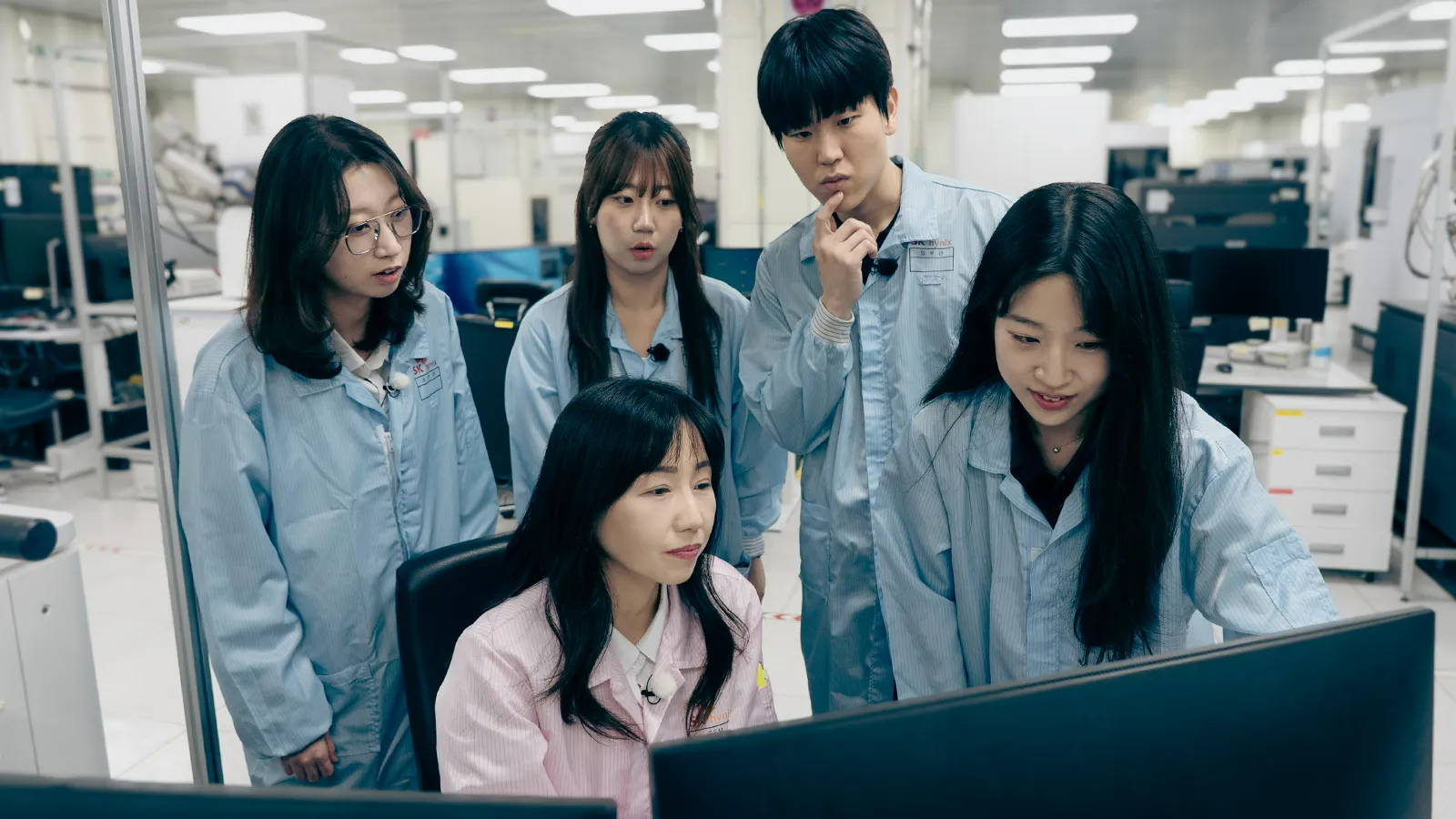
Delivering Both Technological Competitiveness and Manufacturing Efficiency—R&D Process
The core objective of the R&D Process team, which develops advanced technologies related to semiconductor manufacturing, is to develop new processes and equipment that secure both manufacturing efficiency and technological competitiveness. To use a construction analogy, if the Design and Device teams design the building’s structure and shape and determine the necessary materials, the R&D Process team verifies whether that design is buildable and develops specific construction techniques and methods. In other words, the primary role of the R&D Process is to translate and optimize the finalized semiconductor product design into actual manufacturing processes. The R&D Process team is structured around specialized manufacturing steps in the front-end process: Photolithography, Etch, Diffusion, Thin Film, and C&C (Cleaning & CMP). Alongside this, the Process Module Analysis (PMA) role, which analyzes defects occurring during the process to enhance process completeness and product stability, plays a critical part. Additionally, the teams dedicated to developing new technologies, such as Wafer Bonding*, stand as another pillar of the R&D Process team. * Wafer Bonding: A process that precisely bonds different wafers to form a vertical stacked structure. It is a core technology essential for implementing complex integrated structures, such as high-performance AI semiconductors. R&D Process engineers conduct experiments and validations at each process stage to determine the manufacturability of new device structures, securing a consistent level of yield. Once conditions suitable for mass production are established, the technology is transferred to enable the process to be applied to the mass production line, allowing full-scale production to begin.
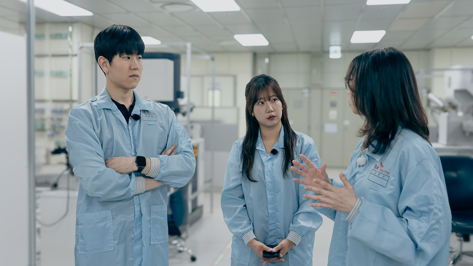
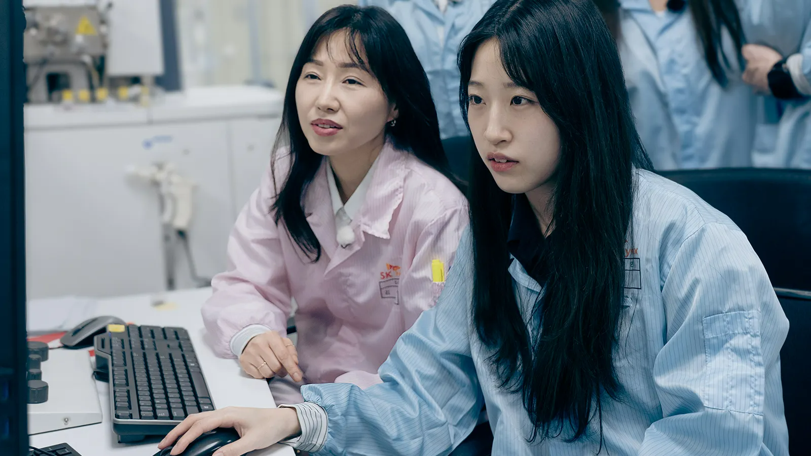
Who We’re Looking For
The R&D Process goes far beyond improving existing processes; it serves as the starting point for advanced research that realizes next-generation semiconductor technology, and acts as the technical hub connecting design, device, and mass production. Therefore, the core competency required for the R&D Process role is having the qualities of a researcher. A broad theoretical understanding of semiconductors and technical knowledge of each process are fundamental. Additionally, problem-solving skills to handle defects or variables, and precise, logical data analysis capabilities based on quantitative evidence, are highly valued. Above all, the ability to continuously learn and explore is essential. As new process conditions, materials, and technologies constantly emerge in the R&D process field, continuous learning and proactive problem solving mindset are needed to keep up with rapid changes. Sangmok Song (TL, Talent Acquisition) emphasized, “The R&D Process is at the frontline of technological innovation in the semiconductor industry. With technological changes like AI and data-based process optimization and new process development to overcome scaling limits, the importance of this role is evolving rapidly.” He added, “Competitive R&D Process talents must have the ability to accurately understand problems, analyze them to set appropriate research goals, and relentlessly find solutions. We encourage applicants interested in developing new technologies or applying developed products to mass production to apply and challenge themselves in this role.”


Q1. Could you briefly introduce yourselves?
Jieun Kim (TL): I work in the N-PMA (NAND Process Monitoring & Analysis) team at the R&D Center. Our team’s main mission is to detect defects occurring in the process early and analyze their causes to reduce the overall product development timeline. Specifically, I handle tasks related to the NAND process. Byul Choi (TL): At the R&D Center, I am developing Wafer Bonding, a new technology to overcome the limits of existing processes. Wafer Bonding involves fabricating only the necessary parts from different wafers and precisely aligning and bonding them to create a new structure. It is gaining attention as a next-generation semiconductor stacking technology.
Q2. How is the work of the R&D Process typically carried out?
Jieun Kim (TL): Process technology development starts with researching and experimenting with core elemental technologies. After securing the technology’s completeness through a Task Force (TF), it is refined into conditions viable for mass production and then transferred to the mass production organization. During this process, our PMA team collaborates closely with the PEDTC (Photo, Etch, Diffusion, Thin Film, C&C) process teams to quickly identify the causes of defects, and we also actively cooperate with the Infra Tech Center to develop analysis methods. Byul Choi (TL): Semiconductor process development requires close collaboration, as various processes are tightly interconnected. This involves not only tracing defect root causes and improving processes but also working closely with equipment vendors to introduce suitable tools and derive optimal conditions. Furthermore, collaborating to transfer the technology to the mass production organization after development is another critical task.
Q3. What do you think is the most important element in performing this role?
Jieun Kim (TL): Because collaboration is involved in every workflow of the R&D Process role, communication skills are extremely important. Furthermore, since experiments must be repeated until the desired results are achieved, perseverance and curiosity are equally vital. Byul Choi (TL): I would choose accuracy and meticulousness. The results of the experiments I conduct will be used as references for follow-up experiments and significantly impact future technology research. Performing every evaluation accurately and meticulously documenting the records is the essential attitude of an R&D Process researcher.
Q4. What advice would you give to prospective applicants seeking a career in R&D Process?
Jieun Kim (TL): If you have ever felt interested in designing an experiment and analyzing the cause and effect, you will be a great fit for the R&D Process role, where you repeat the cycle of testing new technologies, interpreting results, and solving problems. While major knowledge or data analysis skills will help you understand the work quickly, the most important thing is an attitude to learn continuously. Byul Choi (TL): If you are someone who enjoys starting from scratch, you will thrive in this environment. We are a company made up of talented individuals, each contributing in their own unique way. With that in mind, it would be helpful to have a clear understanding of your own strengths and be able to explain how they align with the role.